

What is an Advanced Design System used for?
The Advanced Design System (ADS) is a tool that helps engineers design and test electronic circuits before building them.
Think of it as a virtual lab where you can simulate how different parts of an electronic device will work together.
Engineers harness the power of ADS to create a broad spectrum of products, from simple amplifiers to complex systems like mobile phones, radar, or elements that include high-speed data connections. This versatile tool helps reduce mistakes and ensures everything works perfectly before moving to real-world production, empowering engineers to tackle any design challenge. [2] [3]
What is ADS RF?
ADS RF (Radio Frequency) refers to using ADS software specifically for designing and testing devices that work with radio waves.
This includes gadgets like wireless networks, satellite communication systems, and mobile phones. ADS RF helps engineers simulate how signals move through circuits and ensure they work well at high speeds, which is crucial for modern technologies like 5G. [2] [3]
What does ADS stand for in engineering?
In the field of engineering, ADS stands for Advanced Design System.
It is a software tool that engineers use to design, simulate, and test circuits and systems without first building them.
ADS, an acronym for Advanced Design System, is a pivotal software tool in the field of engineering. Its applications span across industries such as telecommunications, radar systems, and electric vehicles. It plays a significant role in optimizing designs and ensuring performance meets the necessary standards. [3] [2]
What is an ADS system?
An ADS system is a comprehensive software package that equips engineers with everything they need to design electronic products. It provides a one-stop solution, from drawing out circuit designs to running simulations to see how those designs will perform in real life, ensuring engineers are well-equipped for their design tasks.
It provides everything they need in one place — from drawing out circuit designs to running simulations to see how those designs will perform in real life.
It also plays a crucial role in troubleshooting potential issues, such as power loss in high-speed circuits or improving efficiency in power systems like solar inverters and electric vehicles.
With tools for 3D design, electromagnetic simulations, and even artificial intelligence, ADS makes the design process faster and more accurate. [3] [2]
How to Use Advanced Design System?
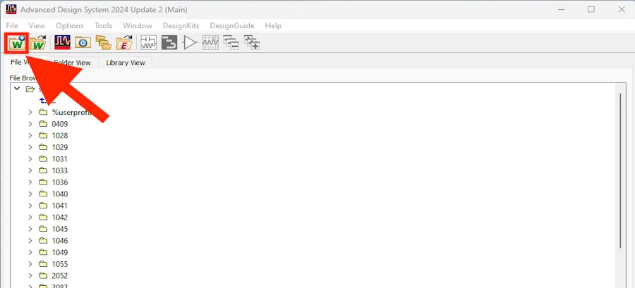
This tutorial will use Advanced Design System 2024 Update 2 to design a passive circuit, such as an RF filter. [1]
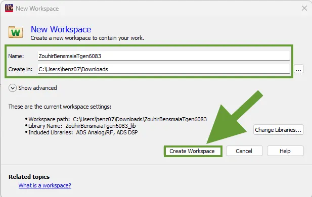
Creating a workspace, and schematic
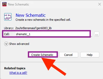
Click where indicated below, then give your workspace a name and choose the path where it will be saved on your computer. Then click "create workspace."
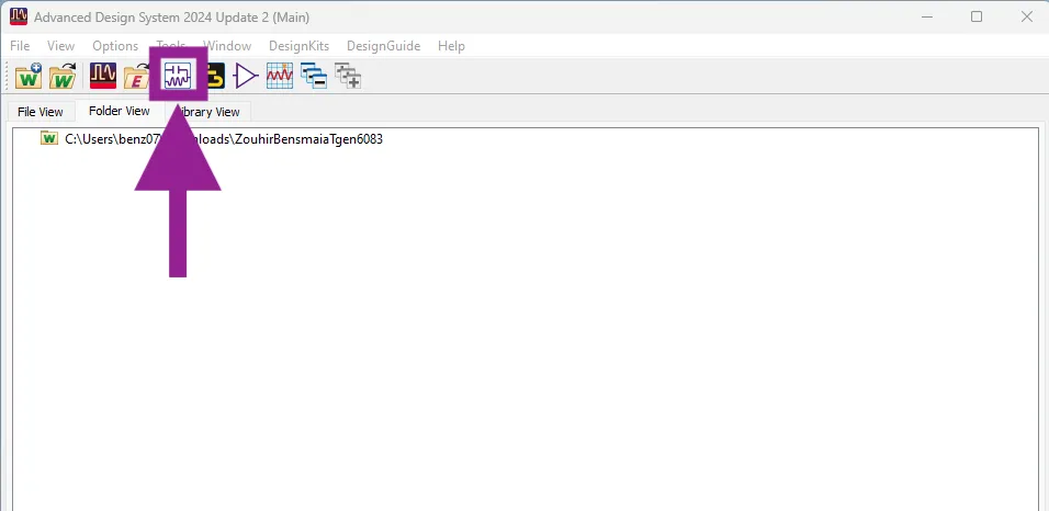
To create a schematic, click as indicated below ("new schematic window").
Give your schematic a name on the new pop-up window, then click "Create schematic." [1]
Advanced design system Example: Design of an RF filter
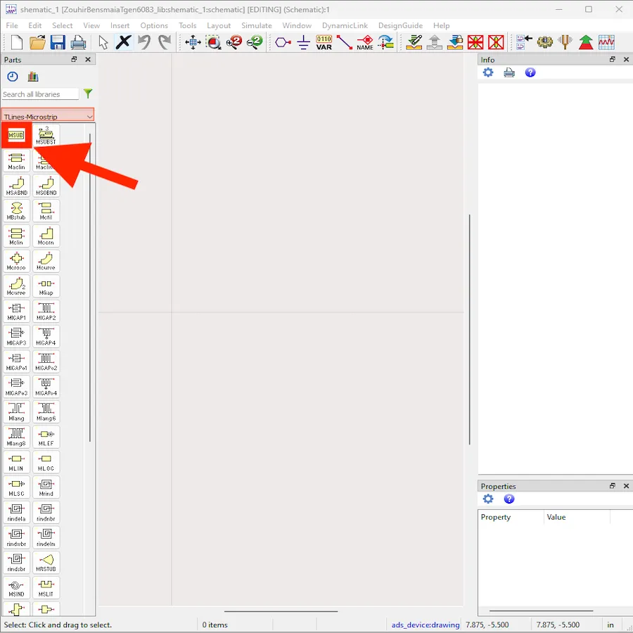
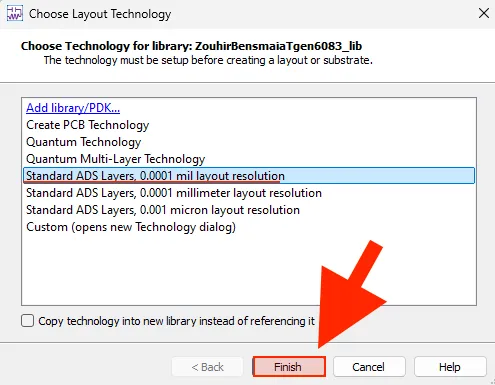
Now that you've opened a fresh schematic canvas, the first step in designing an RF filter (which blocks specific frequencies and lets others pass) is to set up the 'substrate.' The substrate, the base material that holds all the circuit components together, affects how signals travel through the circuit. To set this up, you must add a specific part called MSUB ('microstrip substrate ') from the Tline-Microstrip palette.
You must add a specific part called MSUB ("microstrip substrate") from the Tline-Microstrip palette to set this up.
"Tline-Microstrip" refers to components used in designing electronic circuits, specifically in RF (radio frequency) or microwave circuits. Let's break it down simply:
- Tline stands for Transmission Line. A transmission line is a structure that carries electrical signals from one point to another. It's like a road for electricity or signals to travel through a circuit.
- Microstrip is a specific type of transmission line. It's a flat, narrow strip of metal that sits on a board (usually a printed circuit board or PCB) with a special material (called a dielectric) underneath it. Microstrip lines are widely used in high-frequency circuits like antennas, mobile phones, and satellites because they can effectively carry signals over short distances.
In ADS, the 'Tline-Microstrip' palette is a set of tools or components engineers use to design and simulate microstrip transmission lines in their circuits. It aids in visualizing how signals travel and how different line widths, lengths, and materials affect the signal's behaviour.
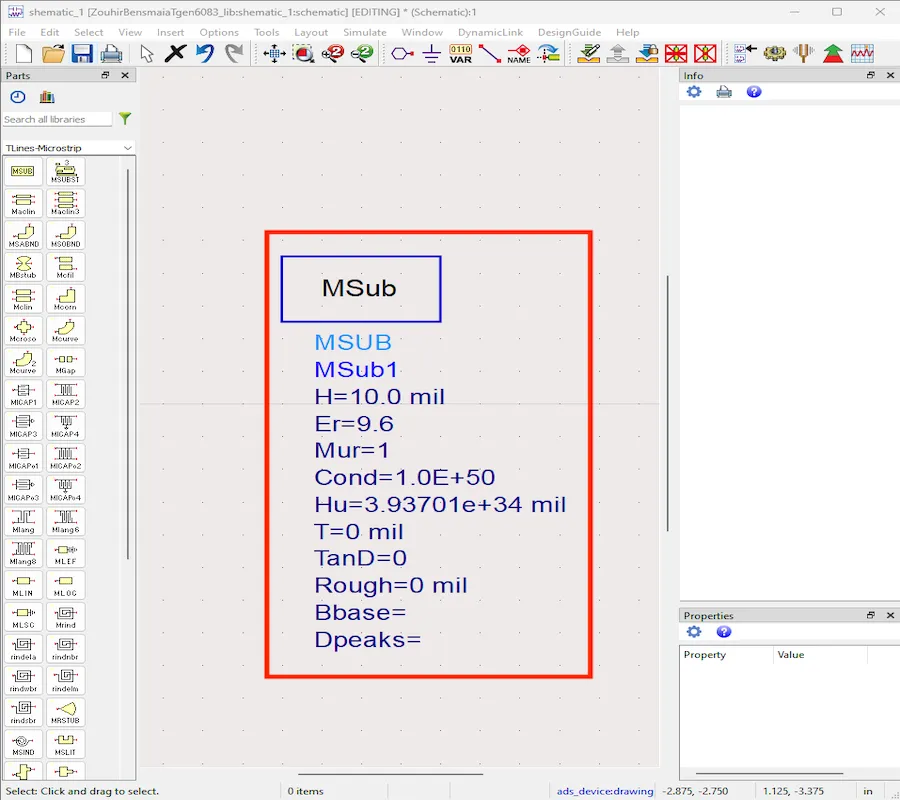
This part allows you to adjust important properties that will affect your design, such as:
- Relative permittivity (εr): This controls how easily electric fields pass through the material.
- Thickness (H): This refers to how thick the substrate is.
- Conductivity of the metal (Cond): This tells you how well the metal used in the circuit will conduct electricity.
- Loss in the dielectric (TanD): This represents how much energy is lost as the signal passes through the substrate.
Adjusting these values allows you to fine-tune your design and achieve the performance you want from your RF filter.
To do so, follow the indications below to generate and set the microstrip substrate with the needed parameters:
Building the Circuit
After setting up the substrate, the next step is to draw the circuit in the schematic window. To do this, you'll use parts from the Tline-Microstrip palette. This palette has different microstrip lines, essentially tiny metal strips on the circuit board that carry signals. You'll be using both MLIN and MCFIL components. These parts represent different microstrip lines used for various purposes in your design.
Once you place a component on the canvas, you can double-click on it to adjust its parameters. For example, you'll need to set each line's width (W) and length (L), which affects how the signals will behave in the circuit.
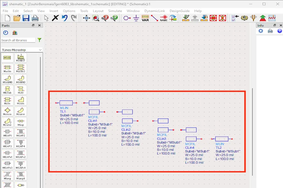
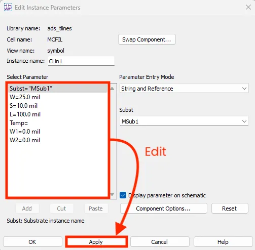
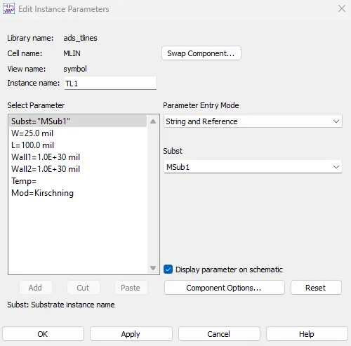
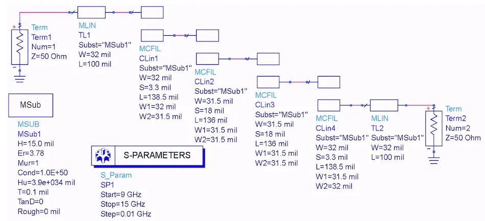
We edit all the parameters to match the reference schematic below:
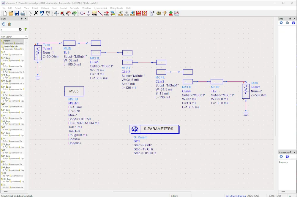
Next, the software will automatically assign ports acting as input and output terminals to ensure your design can be turned into a physical layout (a real-life circuit board). This step ensures a smoother process.
To ensure TL1 is the first component in the signal chain, verify its connection to the input port (Term1) on the left side of your schematic. Signals enter the circuit through this port, and TL1 should be connected directly.
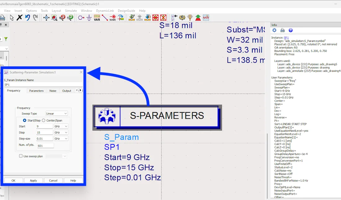
S-Parameter analysis
Finally, you must select the type of analysis you want to perform on the circuit. For this filter design, you are interested in seeing how well the circuit is "matched" to its inputs and outputs (meaning how well the signals can travel without loss). For this, an S-parameter analysis is used. This analysis helps determine how much of the signal is passed through, how much is reflected back, and how much is lost.
The schematic shows the entire filter design aimed at working at 12 GHz (a frequency commonly used in communications). Each circuit part has specific properties like width, length, and the substrate it's built on. The S-Parameter block in the design helps simulate the filter's behaviour to ensure it meets your design goals.
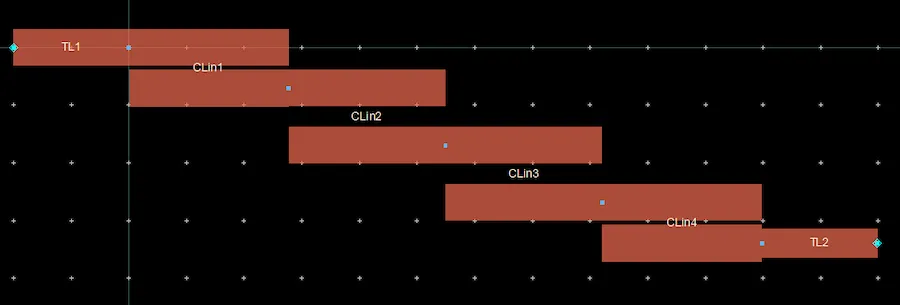
Generating and Visualizing the Physical Layout of the RF Filter Circuit
In this step, the software automatically creates the physical layout of your RF filter circuit. Think of it as the blueprint for your circuit's design when it's built onto a real circuit board.
Here's what is being done, explained:
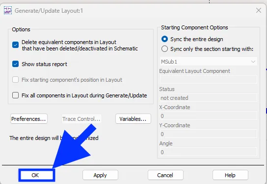
- Layout creation: The layout is generated using a software command called layout> Generate/Update layout. This command converts the schematic (the drawing of how the circuit works) into a physical design that can be printed onto a circuit board.
- Layout visualization: Red rectangles represent your circuit's microstrip transmission lines and components in the image. These shapes show how the circuit will physically look on the board, with each component placed in sequence from TL1 at the beginning to TL2 at the end. The layout ensures all components are positioned correctly so the signals can flow through the circuit without issues.
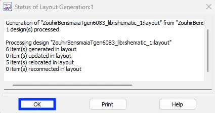
This layout step is essential for preparing the design for manufacture and ensures that the physical connections between components match those planned in the schematic.
Below is an image of the generated physical layout: (click ok when the dialogue box pops up)
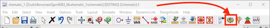
Simulating the Circuit
To simulate the circuit, follow the indications below:
Visualizing the RF Filter Analysis Results
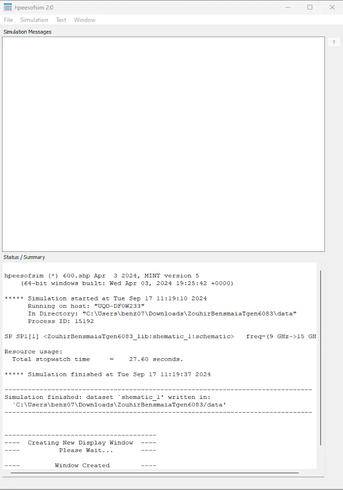
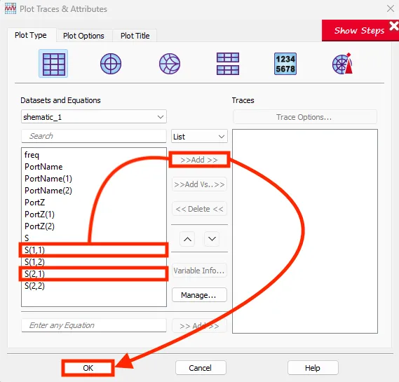
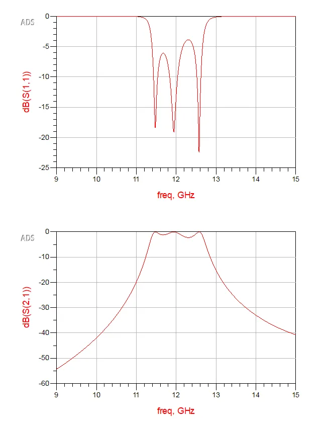
After simulating the circuit, the "New Data Display" window automatically opens, allowing you to visualize the results of your RF filter design. Depending on what kind of information you want to analyze, you can choose different types of plots. For example, you might use a Smith Chart, a polar plot, or a linear plot.
In this case, a linear plot was selected to display the S-parameters (S21 and S11) across different frequencies. The S-parameters help you understand how well your filter passes signals at specific frequencies, which is critical for ensuring your design works as intended.
- S21 shows how much signal passes through the filter (from input to output).
- S11 indicates how much signal is reflected back at the input (which should be minimized).
The graphs show that the filter performs optimally between 11.22 GHz and 12.86 GHz, with minimal signal loss. These points, labelled m1 and m2, help identify the filter's bandwidth and performance, confirming the filter is designed correctly for the target frequency range.
These results are critical because they allow you to fine-tune your design based on real-world simulations, ensuring your circuit works perfectly before you physically build it.
Conclusion
If you're looking for an IT service provider that delivers top-tier web development, AI automation, web design, SEO, and data management expertise, look no further than Earnanswers. Whether you're aiming to enhance your online presence or streamline your business with cutting-edge solutions, our team at Earnanswers has the skills and experience to help you achieve your goals. Contact us today to take your projects to the next level!