

DC Bias Point
This blog article will explore the step-by-step process of designing a Low-Noise Amplifier (LNA) using Advanced Design System (ADS) software.
This detailed walkthrough will serve as a guide to understanding key concepts and techniques necessary for the development of high-performance RF circuits, focusing on active circuit analysis. [1] [2] [3]
Advanced Design System ADS
Before designing a Low-Noise Amplifier (LNA), it's important to familiarize yourself with the Advanced Design System (ADS), the powerful software we'll be using throughout this process. ADS is an industry-standard tool for RF and microwave circuit simulation, and it provides all the necessary features to design, simulate, and optimize circuits like LNAs.
To begin, you'll need to ensure that you have ADS installed and understand its basic functionality, such as setting up schematics, running simulations, and interpreting the results. If you're new to ADS or need a refresher, check out this Advanced Design System Tutorial, which will guide you through the software's essential steps. This tutorial covers everything from navigating the interface to performing advanced simulations, so it's a great starting point for beginners and experienced users alike.
Once you're comfortable with ADS, we can proceed with the specific steps involved in designing an LNA, starting with setting up the circuit and determining the correct bias points for the transistors.
Determination of the DC bias point
One of the most critical steps in designing an LNA is setting the DC bias point for your active component, typically a transistor.
The DC bias point ensures that the transistor operates in the correct region for amplification, providing optimal performance without distortion. In this section, we'll guide you through determining the bias point, which sets up the transistor for proper operation in the active region, balancing performance and stability.
Preparing Design Kits for the Schematic
Before we create the schematic for the DC bias point setup, we must load the necessary Design Kits. These kits contain the models and libraries allowing you to use specific RF transistors and S-parameters in your design. This is crucial for ensuring that your simulation reflects real-world components.
Loading the Design Kits
Unzip the Design Kit
- Navigate to DesignKits > Unzip Design Kit in ADS. This will allow you to unpack and load the necessary models for the transistors and other components you'll be using in your LNA design.
- Ensure the relevant kits are added to your workspace once unzipped.
Add the Design Kit to the Library
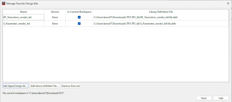
After unzipping, navigate to DesignKits> Manage Favorite Design Kits to ensure the kits are added to your ADS workspace.
The design kits to load include the following:
- RF_Transistors_vendor_kit: This kit provides transistor models specific to RF designs, allowing for accurate simulation of your LNA's active components.
- S_Parameter_vendor_kit: This kit supplies S-parameters, which are essential for understanding how the LNA will perform over different frequencies, particularly regarding gain and impedance matching.
Verifying the Loaded Design Kits
Before proceeding with the schematic creation, double-check that the design kits are properly loaded. As shown in the image, the RF_Transistors_vendor_kit and S_Parameter_vendor_kit should be listed under Manage Favorite Design Kits.
Confirm that they are checked as "In Current Workspace."
If any design kits are missing or not loaded correctly, re-add them using the Add Zipped Design Kit option.
By ensuring that these kits are available, your design will have access to the accurate models needed for simulating real-world components, allowing you to set the appropriate DC bias point for your LNA design.
Setting Up the Circuit for DC Bias Point Determination
In this section, we will break down the components of the schematic and explain their role in determining the transistor's DC bias point. This setup is essential to ensure that the transistor operates in its active region, making it suitable for amplification. Let's go through the circuit parts and the role of key elements like the Parameter Sweep, VAR Equation, and DC Sources.
Circuit Components Overview
- Transistor (Q1 - pb_hp_AT41411_19921101): this is the Bipolar Junction Transistor (BJT) used in this design. The DC biasing process aims to set the appropriate collector-emitter voltage (VCE) and base current (IBB) so that the transistor operates optimally in the active region.
- DC Source (V_DC - SRC3): VCE Source: This DC voltage source applies a variable collector-emitter voltage (VCE) to the transistor. The variable VCE is swept across different values in the simulation to determine how the collector current (IC) changes with VCE.
- DC Current Source (I_DC - SRC2): IBB Source: This current source applies a base current (IBB) to the transistor. The Parameter Sweep will vary the base current to simulate how different IBB values affect the collector current (IC) and VCE relationship.
- Current Probe (I_Probe): This probe measures the collector current (IC). It tracks the IC values as the VCE and IBB are varied during the simulation. The results show how the transistor responds to different biasing conditions.
Key Simulation Elements
Parameter Sweep Block
The Parameter Sweep block is crucial because it allows us to automatically sweep through different base current (IBB) values during the simulation. In this case:
The base current (IBB) is swept from 5 µA to 30 µA in steps of 5 µA. This allows the simulation to capture the transistor's behaviour over a range of IBB values.
The SimInstanceName links this sweep to the correct simulation instance (DC1), ensuring the sweep is applied properly during the DC analysis.
VAR Equation Block (VAR1)
The VAR Equation block defines variables for the simulation. In this case:
IBB = 0 A
VCE = 0 V
These are the initial values of the base current and collector-emitter voltage, respectively. The sweep will modify these values during the simulation, but this block helps initialize and define them in the schematic.
DC Simulation Block (DC1)
This block instructs the software to perform a DC analysis of the circuit. The DC simulation calculates the steady-state (DC) values of currents and voltages throughout the circuit.
Impact on Simulation: This is the core of the analysis. The DC block ensures that the circuit is analyzed regarding how IC changes concerning VCE and IBB under DC conditions. The results will help determine the transistor's behaviour at different operating points. The DC Source will set VCE as the sweep parameter and will vary from 0 to 3 V with a step of 0.1
How This Setup Affects the Simulation
By combining the Parameter Sweep (to vary IBB) and the DC simulation (to analyze IC vs. VCE), we can plot IC vs. VCE for different base current values.
This setup allows us to identify the transistor's DC bias point, which is crucial for ensuring optimal performance in real-world applications such as low-noise amplification.
The DC sources ensure that appropriate voltages and currents are applied, and the current probe allows us to measure and visualize the results.
By understanding how these components interact in the simulation, we can optimize the transistor's bias point and ensure it operates effectively as an amplifier.
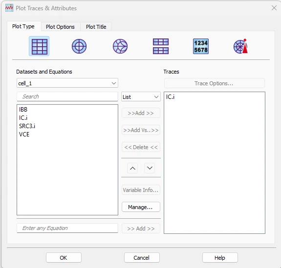
We Execute the simulation and then plot the IC vs VCE for swept values of IBB and VCE.
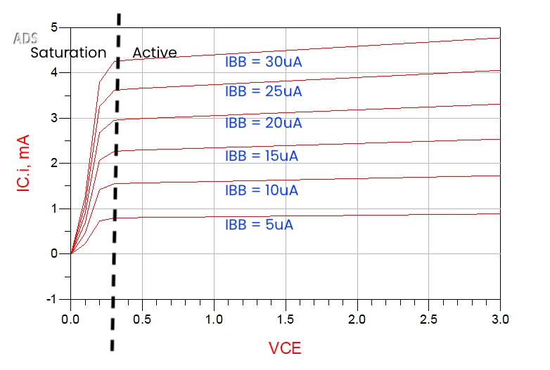
Analyzing the I-V Characteristics of the Transistor
In this section, we'll analyze the transistor's I-V characteristics, as shown in the graph. The graph plots the collector current (IC) against the collector-emitter voltage (VCE) for different values of base current (IBB). Each curve represents a different base current value, and we will explore the key insights this provides regarding the transistor's behaviour in different operating regions.
Key Observations and Analysis
Saturation Region (VCE < 0.3V)
In this region, for very low values of VCE (close to 0V), all curves show a rapid increase in IC. This indicates that the transistor is operating in the saturation region.
In this region, the transistor behaves like a closed switch, and the collector current is mainly determined by the base current (IBB), with very little dependence on VCE.
Active Region (VCE between 0.3V and 3V)
Beyond approximately 0.3V, the curves flatten out, indicating that the transistor has entered the active region.
In this region, IC is primarily controlled by IBB and becomes relatively independent of VCE. This is the ideal region for amplification because changes in VCE have little effect on the current.
The flatness of the curves shows that the transistor is operating as an efficient amplifier, which is where you want it to be for low-noise amplification.
Linear Increase in IC with IBB
As IBB increases (from 5 µA to 30 µA), each curve shifts upward, indicating that increasing the base current leads to a higher collector current. This linear relationship between IBB and IC is crucial for designing amplifiers, as it allows small changes in IBB to control larger changes in IC.
Saturation Point
The transition between the saturation and active regions occurs around VCE = 0.3V. This is where the transistor moves from behaving like a switch to functioning as an amplifier.
Optimal Base Current (IBB)
The base current values (IBB) range from 5 µA to 30 µA. The choice of IBB for the LNA design will depend on the desired operating point. A higher IBB leads to a higher IC, meaning more gain and increasing power consumption.
For most designs, you'll want to choose an IBB that ensures the transistor operates in the active region (VCE > 0.3V) while providing sufficient collector current for amplification without excessive power dissipation.
Collector Current (IC)
In the active region, the collector current ranges from ~0.5 mA (at IBB = 5 µA) to ~4.5 mA (at IBB = 30 µA). The desired value of IC will depend on the amplifier's power and gain requirements.
Typically, you want a current high enough for significant amplification but low enough to avoid unnecessary power consumption.
Optimal Biasing in the Active Region
You want to ensure the transistor operates in the active region with a VCE higher than 0.3V. This ensures that IC is primarily controlled by IBB, making the transistor a reliable amplifier.
Choose an Appropriate IBB
The IBB should be chosen based on the required gain and power considerations. A higher IBB will provide more gain (higher IC) but with higher power dissipation.
Avoid Saturation
Refrain from operating in the saturation region, as this would reduce the amplifier's effectiveness by making IC too dependent on VCE.
Conclusion
This graph provides crucial insights into the transistor's behaviour in different operational regions. For optimal performance in an LNA, you want to bias the transistor in the active region, where IBB controls IC primarily. The key is to choose the correct values for VCE and IBB to achieve efficient amplification with minimal noise and power consumption.
For more advanced design techniques, be sure to read our next blog in this series, "Optimizing Transistor DC Biasing with Advanced Design System ADS", where we dive deeper into further optimization methods and practical LNA design tips.