
How to Design a Active Circuit Low-Noise Amplifier LNA Using Advanced Design System ADS
If you're interested in learning more about transistor circuit design and optimization, be sure to check out part 1 of this series: "How to Design an Active Circuit Low-Noise Amplifier (LNA) Using Advanced Design System (ADS)", where we dive into the basics of low-noise amplifier design with detailed explanations and ADS simulations. [1] [2] [3]
Definitions: DC Biasing, Bias Point, Optimization Cockpit and Biasing Network
DC Biasing:
DC biasing provides a steady, unchanging direct current (DC) voltage to an electronic component like a transistor to ensure its proper operation. In the case of a transistor, DC biasing helps set the conditions so that the transistor can effectively amplify signals without distorting them.
Consider DC biasing as setting a steady baseline or starting point for a transistor, much like warming up a car's engine before driving. It makes sure everything is ready for the transistor to amplify incoming signals.
Bias Point:
The bias point (the operating point) is the specific current and voltage we apply to a transistor or other component to ensure it functions correctly. This point is carefully chosen so that the transistor operates in the active region—the sweet spot where it can amplify signals without cutting them off or saturating them.
Imagine the bias point as the perfect balance on a see-saw. If there is too much weight on either side (too high or too low voltage/current), the balance is lost, just like a transistor would only work properly if its bias point is set correctly.
Optimization Cockpit:
The Optimization Cockpit in ADS is like a control room where we can automatically adjust certain settings, like resistor values in a circuit, to meet specific goals. For example, if we want the transistor to have a certain voltage or current, the Optimization Cockpit helps tweak and fine-tune those values through multiple iterations until everything is correct.
It's similar to using an app that helps you adjust various settings on a device until they reach the desired outcome—except, in this case, it's doing it for an electronic circuit.
Biasing Network:
A biasing network is a group of components—usually resistors—that work together to provide the correct DC biasing to a transistor. This network sets the proper conditions for the transistor to function by controlling the voltage and current. It's like a system of gears that ensures everything runs smoothly in a machine.
In simple terms, consider the biasing network as the ingredients you add to a recipe to get the right flavour. Each component (resistor, capacitor, etc.) ensures the transistor has the right "flavour" of current and voltage.
Determination of the Biasing Circuit
In transistor-based designs, determining and optimizing the bias point is crucial for ensuring the device operates efficiently. We begin by setting up the bias point for the transistor in ADS (Advanced Design System). The goal is to establish a steady direct current (DC) to drive the transistor in its active region for adequate amplification.
To ensure that the transistor operates correctly in the desired region, we will adjust resistances and other parameters in the biasing network and use the Optimization Cockpit in ADS to fine-tune the design.
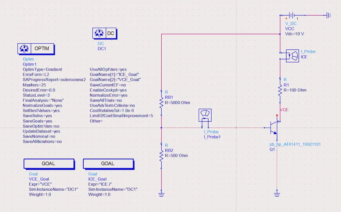
Initial Setup for Bias Point Determination
The first step is creating a basic schematic to determine the bias point. As shown in the image below, the schematic includes:
- A DC voltage source for the collector-emitter voltage (VCE).
- A current source for the base current (IB).
- Two probes measure the collector current (IC) and VCE.
We aim to achieve VCE = 8V and IC = 24.35 mA as initial design targets. To achieve these values, we must carefully select resistor values in the biasing network.
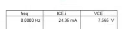
Pre-Optimization Results
Before running the optimization, ADS provides the initial results for IC and VCE. The table below shows that the initial values are IC = 24.35 mA and VCE = 7.565 V. While these values are close to our targets, further optimization is necessary to refine the bias point for better performance.
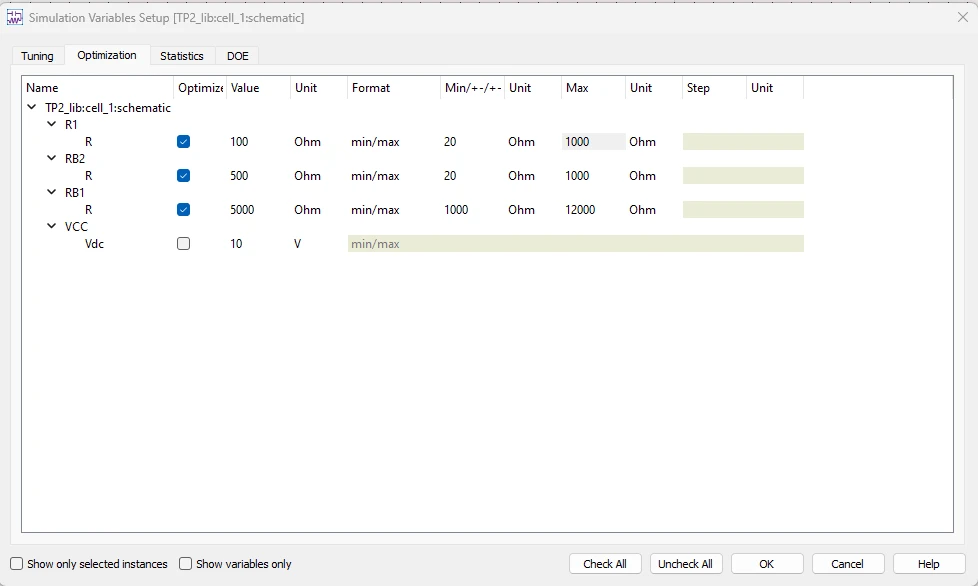
Simulation Variables Setup
Next, we must configure the simulation variables to allow ADS to optimize the resistor values. As shown in the image below, the resistors R1, RB1, and RB2 will be adjusted during optimization. The ranges for each resistor are set, allowing ADS to explore different values to meet the design goals.
This setup provides flexibility in adjusting the bias point without requiring manual intervention, which is crucial when tuning the circuit for specific voltage and current values.
The next step involves using the Optimization Cockpit to fine-tune these values and achieve closer alignment with the design goals.
Utilizing the Optimization Cockpit
The Optimization Cockpit in ADS allows us to adjust and fine-tune the resistor values in the biasing network to meet the design goals for IC and VCE. The Image displays the Optimization Cockpit after running a few iterations.
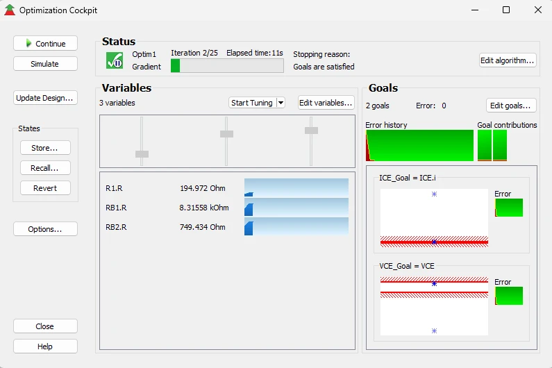
The system used a Gradient algorithm to adjust the resistor values R1, RB1, and RB2, eventually minimizing the error to zero. The goals for IC and VCE were successfully met after 2 iterations, as shown in the cockpit interface.
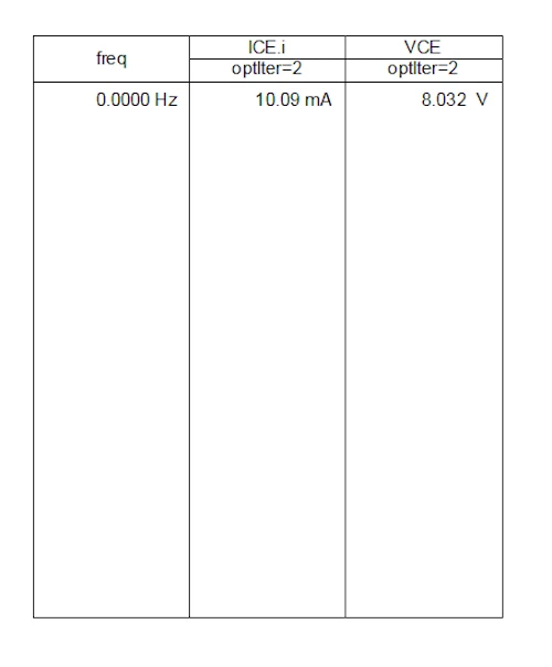
Post-Optimization Results
After optimization, the results can be viewed in graphical and tabular form. The image below shows the post-optimization voltage and current values plotted over frequency.
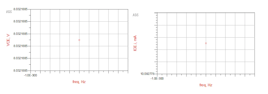
The optimized current (IC) and voltage (VCE) are shown to be close to the target values after the optimizer's adjustments.
Lastly, the image below shows the tabular post-optimization values for IC and VCE.
After optimization, the IC settled at 10.09 mA, and the VCE was now at 8.032 V, achieving the desired performance for the transistor's operation.
Conclusion
For more advanced design techniques, be sure to read our next blog in this series, Template Name #, where we will explain how to perform stability analysis to ensure the amplifier remains stable across the desired operating frequency range.